"Wood chips" takes on new meaning with a new green technology, cellulose nanofibril, or CNF, developed by researchers at the University of Wisconsin-Madison and the U.S. Department of Agriculture Forest Products Laboratory and detailed in a research paper published this week in Nature Communications.
The "chips" in question are indeed made mostly of wood -- but they are also computer chips.
As of 2007, about 3.2 million tons of electronic waste was being generated each year, the researchers noted. Again, that was eight years ago.
The good news is that in leveraging the promising principles of nanotechnology, the researchers proposed that CNF can alleviate the strain electronic waste places on the environment.
Don't Knock Wood
Most of a computer chip's material is designed to support the tiny transistors and calculator, according to Zhenqiang "Jack" Ma, University of Wisconsin professor of engineering and study author. Everything else accounts for only a few micrometers.
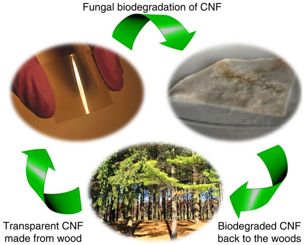
Paper is the most common product processed from wood fibers. Those fibers are what Ma called the "micron stage." But what if researchers went further?
When those fibers are broken down to the nanoscale, they can form "very strong and transparent CNF paper," said Ma.

Most other substrates for computer chips are derived from petroleum polymers, with half lives that indicate they can survive for generations. On the other hand, fungal colonies would feast on tech that employed CNF -- but that's also one of CNF's vulnerabilities, according to Ma.
"If the CNF is not sealed well, fungi may attack it," he said.
There are a great many potential use cases for such material, many of which would entail replacing nonbiodegradable substrates.
CNF "can be used for many things, including mobile devices, displays, solar cells and much more," Ma told TechNewsWorld.
However, it will be up to governments and other large investors to push CNF into fruition, he added.
"CNF is eco-friendly and is suitable for many of today's electronics applications besides other potential applications," he noted, but "governments may need to provide some incentive to encourage industry to adopt it."
Nanotechnology's Promise
While it may be a while before the researchers' CNF designs hit mass production, the technology "holds great promise," said Susan Eustis, president of WinterGreen Research.
Biodegradable tech could outpace environmentally harmful electronics "within 10 years," she estimated.
"Quite soon, we'll see about 60 percent of our tech [composed of sustainable material]," Eustis told TechNewsWorld. "That'll be facilitated by a huge breakthrough in nanotechnology, however."

That significant leap will come soon, Eustis predicted, noing that the sector has been struggling with migrating lab findings to mass production.
"It often works great in the lab, but it's been difficult to commercialize some of the breakthroughs they find, due to a lot of manual processes that they use in the lab," she explained. "In part, those struggles arise because they didn't pick the right nanoparticles to work with."