Worries over the imminent death of Moore's Law have apparently been greatly exaggerated. At least that is the word following announcements on Saturday from both IBM and Intel that each has developed a new energy-saving microchip design. According to the two chip makers, the advance is the biggest breakthrough in chip technology in 40 years.
"Until now, the chip industry was facing a major roadblock in terms of how far we could push current technology," Dr. T.C. Chen, vice president of Science and Technology at IBM research said in a statement. "After more than ten years of effort, we now have a way forward. With chip technology so pervasive in our everyday lives, this work will benefit people in many ways."
It's Alive
Developed four decades ago by Intel Co-Founder Gordon Moore, Moore's Law is a theory that has served as the guiding principle of chip design. It states that the number of transistors on a chip will double in each subsequent generation, or roughly every 18 to 24 months.
Moore's theory has held true until the 1990s, when chip producers started to make a hard choice between energy efficiency and cost. To be cost effective, manufacturers found that the more diminutive the chip and the more transistors it contained, the more power leakage occurs. As computer chips have grown smaller and more compact, chip designers and manufacturers have feared that the increased cost and lack of energy efficiency would mean the end of Moore's Law.
"As more and more transistors are packed onto a single piece of silicon, the industry continues to research current leakage reduction solutions," Mark Bohr, Intel senior fellow, stated.
Metal Heads
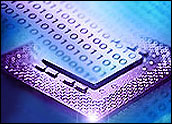
The new Intel and IBM designs are both based on the use of a metallic material known as "high-K." The new metal will be used to build transistor gate dielectrics. Transistors are the tiny switches that are used to sort out the series of ones and zeros that are the foundation of modern computers. The gate shuts the transistor on and off and the gate dielectric, underneath the gate, insulates it by separating it from the channel where current flows.
Unlike silicon, the substance of choice for four decades, building the insulating walls and switching gates of transistors out of the new metal significantly reduces power leakage. The high-K metal gate technology combines the use of high-K for gate dielectrics with a new combination of metal materials to build the transistor gate electrode. That, said Gartner Analyst Dean Freeman will extend Moore's law for several more generations, or about six more years.
"By going to a 'high-K' dielectric and a metal gate," Freeman explained, "this enables you to continue to scale or shrink the transistor for at least two more generations. We are at 45 [nanometers], so then we go to 32, then we're going to 22."
"The implementation of high-K and metal materials marks the biggest change in transistor technology since the introduction of polysilicon gate MOS transistors in the late 1960s," said Intel's Moore.
Evolutionary, Not Revolutionary
The new technology is significant, said Tom Halfhill, an analyst at In-Stat, but is not a revolutionary breakthrough. Engineers have been talking for a long time about metal gates and the need for better gate insulators. According the Halfhill, the development is an evolutionary advance along the lines of others that have occurred in recent years, such as silicon-on-insulator (SOI) transistors, strained silicon and the replacement of aluminum wiring with copper.
"None of these improvements were revolutionary breakthroughs either, but they helped keep the progress of semiconductor technology roughly on track with Moore's law," Halfhill explained.
IBM, which is conducting its research with partners AMD and Toshiba, says it will be 2008 before it begins producing 45-nanometer chips based on the new technology.
For its part, Intel said that it will incorporate the new design the next generation of Intel Core2Duo, Core2Quad and Xeon families of microprocessors, scheduled for release later this year. Consumers will more than likely see the chips in PCs just in time for the 2007 holiday season. The company also expects to include the new chips in a new 45nm line of processors codenamed Penryn. Those chips, targeted at computers running Windows Vista, Mac OS X, Windows XP and Linux operating systems, will begin production in the second half of 2007.
The chips' impact on the market could mean, for instance, that server farms which are notorious power hogs could consume less power, Gartner's Freeman said. "The power leakage through the gate dielectric won't occur. So now, [businesses] can take a 45 nanometer MPU, plug it into a server, and plug that into the server farm without having to make any changes in the overall energy consumption or flow of that server farm."
"In that aspect it is a big leap forward," he continued "because if you had used conventional technology and then pushed it forward, you would have had to increase your thermal budget and thus your heating/air conditioning at your server farm."