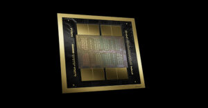
Researchers at IBM have moved a step closer toward the creation of an on-chip optical network, the tech giant said Monday. Calling it a “significant advance,” IBM announced the development of the world’s tiniest nanophotonic switch designed to route optical data between cores on next-generation high-performance multi-core microprocessors.
With the technology, computer chips will one day send information using light pulses rather than electrons, which will significantly boost chip performance and at the same time reduce energy usage. This will make it possible to transmit massive amounts of data simultaneously to multiple cores using roughly 10 times less power and generating substantially less heat than multi-core chips today.
Ray of Light
The scientists’ findings, published in the journal Nature Photonics, are the latest in a series of advancements in on-chip optical networks announced by IBM since November 2005. The silicon broadband optical switch is an essential component in the creation of on-chip optical interconnects.
Once the electrical signals have been converted into pulses of light, the switch assumes a role comparable to a traffic cop within the network, ensuring that optical messages from one processor core can efficiently get to any of the other cores on the chip, IBM said.
Think of it as similar to a light switch — the nanophotonic switch uses light to turn power on or off up and down the stream, said Ian Lao, an analyst at InStat.
“The significance of it is that when you do this using silicone or copper as the substrate, the problem is that copper just can’t transmit the data fast enough. And it’s hot — it generates a lot of heat. When you transmit things using light you can send information back and forth on cores on a processor that are in the radio frequency range. You’re talking gigahertz of processor speed,” he explained.
IBM’s nanophotonic switch can route huge amounts of data using different wavelengths or colors of light simultaneously, the company noted. Each wavelength is capable of carrying data at up to 40 GB/s, making it possible to switch an aggregate bandwidth exceeding 1 Tb/s — a necessity when routing large messages between distant cores.
While this technology has existed for some time, IBM researchers have managed to whittle it down so that this component alone has a footprint that is roughly 100 times smaller than the cross section of a human hair. Its diminutive size means that as many as 2,000 switches could fit side-by-side in an area one square millimeter in size, thus easily meeting integration requirements for future multi-core processors, according to IBM.
Beam Me Up
According to Lao, loss of information and overheating are key problems researchers working on multiple core chips have struggled with.
“Anything that will help that is a benefit. IBM is showing this technology off as a way for semiconductor manufacturers who license this technology to be able to increase the throughput of their processor design. That’s the concept behind it,” he told TechNewsWorld.
The processors are the most hungry now, and with dual core, triple core and quad core chips, processors have to talk not only to the memory and the video — they also have to chat amongst themselves, Lao continued.
“That’s where these kind of things come into play. That cross-talk among the cores is a limiting factor. If I have information I’m foaming at the mouth to deliver to my fellow cores but I have to wait because there is something else going on on the bus, I’m artificially lowering my performance,” he added.
One example, IBM’s Cell processor, which powers Sony’s PlayStation 3 game console, has nine cores on a single chip. As demands for greater computing performance increase, chip designers will boost the number of cores on a chip to the tens or even hundreds of cores, IBM said.
“IBM Cell processor is a high performance chip with a lot of operations per second going on. To scale it to even higher performance, we need a lot of advances in many different areas, and this is how to keep up with the amount of information flowing there and how to make it possible to uses optics and nanophotonics,” Yuri Vlasov, manager of silicon nanophotonics at IBM’s TJ Watson Research Center, told TechNewsWorld.
Vlasov expects the technology to appear in high-performance computers such as Blue Gene in the next five years or so.
“For the big super server guys that have oodles and oodles of cores, they will benefit first,” Lao noted.
The technology could trickle down to consumers in the form of PCs and handheld devices within the next 10 years or so, depending on the costs of the technology.
“It will take a while for us to see it in the main PC lines. Consumers will most likely see the technology on the back-end with server farms set up by Google, Yahoo, etc., that service all the requests to the Internet. This technology will affect that area first and lead to a faster Internet experience,” he said.


