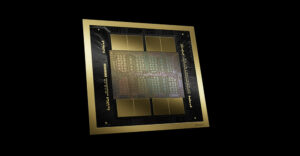
An industry consortium that includes IBM, Chartered Semiconductor, Infineon and Samsung said this week they plan to make available the first silicon-functional circuits and design kits for 45-nanometer low-power process chip technology.
The 45nm manufacturing process shrinks the gap between transistors on each chip further from 65nm and allows manufacturers to pack more transistors onto the devices. This makes possible more powerful chips that offer increased performance, improved memory and other advanced features for computers and a multitude of other electronic devices.
Working Together
The consortium said its working circuits based on 45nm technology were aimed at next-generation communication systems, and that the design kits draw on all four companies’ expertise.
Wide production of chips using 45nm technology should be under way in about a year, the companies said.
“It’s a major coup in that the alliance shows that it’s working,” Semico Research Managing Director of Manufacturing Joanne Itow told TechNewsWorld. “It shows it doesn’t have to all come from individual companies investing huge amounts of money.
“When you put out a prototype and you’ve got product production at the end of 2007, you’re in the big leagues,” she noted.
Valuable Partnership
The consortium’s body of work incorporates technology contributed by each member as well advances that have come out of members’ partnerships with other firms, such as Big Blue’s cooperation with Advanced Micro Devices. The group’s silicon-functional circuits, characterization of key design elements in silicon and early design kits will provide other chip designers a fast track in advancing to the smaller, more efficient 45nm technology.
“The speed, innovation and completeness with which this first 45nm offering has been developed and made available to customers demonstrates the growing customer value and strength of the partnership between these four companies,” said Lisa Su, vice president of semiconductor research and development at IBM and head of the alliance.
The companies said the new 45nm process was tested at IBM’s East Fishkill, New York, facility using 300-millimeter silicon wafers. Other features of the chips included standard library cells, input/output (I/O) elements and embedded memory developed by the alliance.
Tiny, Complex
Chip manufacturers have gone from developing their own process technology and working in a fabless model through outsourcing, to cooperating on technology that is becoming ever more complicated as it shrinks, Mercury Research President Dean McCarron told TechNewsWorld.
“Now, it’s getting so hard that everybody works together on it,” he said.
Computer and electronics makers are dependent on processor improvements such as smaller circuits to improve their own products, said McCarron, who described the manufacturing process as the “engine” that drives the industry.
“The way that improvement is done, ultimately, is through process technology,” he said.
The consortium companies, as well as the wider industry, stand to benefit from the partnership through lower costs and higher volumes, said McCarron.