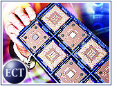
Eastman Kodak and IBM will team up to develop new image sensors for digital cameras and camera phones, Kodak said in a statment.
The agreement seeks to combine Kodak's image sensor technology with IBM's complementary metal oxide semiconductor (CMOS) processing expertise. Kodak hopes to use the technology to bring out a new family of CMOS image sensor (CIS) devices.
The companies say that the new sensors will allow for improved image quality and more innovative features.
The companies did not disclose the terms of the agreement.
The Eye of the Camera
Kodak finds itself in competition with Sony, Samsung and other Asian camera makers, many of which build their own chips. Collaboration with IBM will ensure that Kodak has a guaranteed supply of chips for its cameras and camera phones.
IBM, for its part, gains a strong foothold in the burgeoning consumer digital imaging market. As part of the agreement, IBM will be allowed to sell the chips to customers other than Kodak.
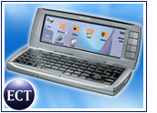
Image sensors act as the "eye" of a digital camera by converting light into electric charges. Digital cameras and camera phones are two of the fastest growing segments of the market for digital imaging. According to Kodak, CIS devices are ideal for this market because they allow simpler designs and draw less power.
Higher Quality Images
CIS devices currently on the market, Kodak says, often fall short of the image quality customers have come to expect from digital devices that use traditional CCD image sensors. The company claims that its new devices will improve image quality and take advantage of the power, integration and cost benefits of CMOS-based sensors.
"Worldwide demand for image sensor devices is expanding at an explosive pace," said Chris McNiffe, general manager of Kodak's Image Sensor Solutions business.
"Today, Kodak is a worldwide leader in charged coupled device (CCD) image sensors serving the high-performance needs of the professional and industrial imaging markets," he said. "Our partnership with IBM now allows Kodak to deploy our core competencies in image science and sensor research into high-volume consumer applications, thereby significantly expanding the market opportunities for our products."
A key element of the joint Kodak/IBM CIS process is Kodak's CIS pixel technology, including its proprietary pinned photodiode and 4T cell architectures. These technologies, licensed to IBM as part of this agreement, permit the manufacture of CIS pixels that approach the size of the smallest CCD pixels offered today, with improved photosensitivity and lower noise.