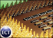
IBM, Sony and Toshiba are launching a new phase of their joint technology development alliance that will lead to the development of advanced process technologies at 32 nanometers and beyond.
Specifically, they are working on further developing the "cell" microprocessor design and its underlying silicon-insulator (SOI) process technologies in 90- and 65-nanometer systems.
Translated into English, this means they want to improve upon and develop practical applications for their networking chip.
"A chip is just a chip until you know how to use it right," Richard Doherty, director of engineering at Envisioneering Group, told TechNewsWorld.
To get its maximum benefit, the cell chip is supposed to be used in a networking environment, he said. "It is a 'neighborly' or 'societal' chip in that it presumes there are other devices in the system." By contrast, a PC chip is used in computers and assumes there is only occasional need to interact with other devices.
New Blood
The next phase of research should yield significant results for this technology, which has been exploited only on a limited basis until now.
"This new commitment to the chip will result in more training, for starters," said Doherty, who has spoken with engineers at some of the companies involved. It will lead to additional internships at IBM, for example.
"You need to have fresh blood looking at chip technology and how it can be applied," Doherty remarked.
Cell chips have been incorporated in processor boards manufactured by Mercury Computer Systems, which are used by the Department of Homeland Security and for medical diagnostics.
Also, Sony has committed to using the cell chip for PlayStation 3, according to Doherty, which is supposed to start shipping this spring.
Cell phones are not likely to incorporate these chips for five years, however.
From Research to Commercial Applications
"The extension of the IBM, Sony and Toshiba relationship to fundamental research is extremely promising," said Kenshi Manabe, president of EVP's semiconductor business unit and corporate executive of Sony.
"This joint development project will help accelerate the cycle from fundamental research to commercialization based on detailed feasibility studies of potential technologies, device structures, innovative materials and unique processing tools," Manabe noted.
Research and development will take place in New York at IBM's Thomas J. Watson Research Center in Yorktown Heights, the Center for Semiconductor Research at Albany NanoTech, and at IBM's 300-millimeter manufacturing facility in East Fishkill.


Heres why I believe "cell" processor will lead to better computing. Its AM ount of data within 64 bit string bitwidth that is important here, plus number of vores in use. Intel uses 40 bitwidth, AMD uses 48 bitwidth & IBM is about to start using 52 bit bitwidth. It sounds like small difference, yet when you multiply 52 bits times 8 cores running together you get 416 bits PROCESSED in same time Intel gets only 40 bits processed 368 more bits processed from 64 bit strings. Or about 8 to 10 times more data processing than single core Intel or AMD. Also IBM uses thier own version open sourced software (linux?) to enable multi core much more effectively, (at least in theory). So IBM has quite advantage in technology, especially by using "cell" in such dedicated & resourceful ways to start.($$$) Eventually 8 core will migrate to all processors & "cell" will be only 80% faster than intel.Signed:PHYSICIAN THOMAS STEWART VON DRASHEK M.D.